P1 connects to the PC parallel port. |
Pin # | Board Marking | Signal |
1 | A0 | Axis 0 A |
2 | B0 | Axis 0 B |
3 | Z0 | Axis 0 Z (index) |
4 | A1 | Axis 1 A |
5 | B1 | Axis 1 B |
6 | Z1 | Axis 1 Z (index) |
7 | A2 | Axis 2 A |
8 | B2 | Axis 2 B |
9 | Z2 | Axis 2 Z (index) |
10 | A3 | Axis 3 A |
11 | B3 | Axis 3 B |
12 | Z3 | Axis 3 Z (index) |
13 | Ground | |
14 | + 5 V |
P2 connects to the PWM amplifiers, and also provides unregulated power to the board, and regulated +5 V can be taken from the board to supply encoders. J2 parallels the connections available on P2 except for the unregulated power input. The PWM signal is zero Volts for "power off" and 5 V for "power on". The driving software could make the PWM waveform operate in the inverted manner, but the E-stop condition will always default to zero Volts. If driving opto-coupled amplifier inputs, connect the + amplifier input terminal to pin 3 (+5 V) and the - input to the PWM or direction pin. If this connection is the wrong polarity, and the amp cannot be switched to invert the sense of the PWM or direction inputs, then you can connect the + to the PWM or direction output and the - input to pin 4 (ground). This should still give sufficient current drive to most opto-couplers. Pins are as follows : |
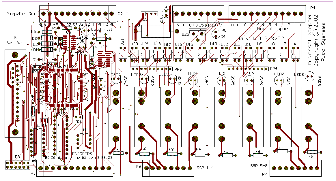
P2 Pin # | J2 Pin # | Board Marking | Signal |
1 | 1 | S0 | PWM to Axis 0 |
2 | 2 | D0 | Direction to Axis 0 |
3 | 3 | S1 | PWM to Axis 1 |
4 | 4 | D1 | Direction to Axis 1 |
5 | 5 | S2 | PWM to Axis 2 |
6 | 6 | D2 | Direction to Axis 2 |
7 | 7 | S3 | PWM to Axis 3 |
8 | 8 | D3 | Direction to Axis 3 |
9 | 13 | G | power ground (same as P2-11) |
10 | 14 | +5 | +5 Volt output |
11 | G | power ground | |
12 | PWR | Unregulated power in |
P4 Pin # | J4 Pin # | Board Marking | Signal | Function |
1 | 1 | 0 | Bit 0 input | X Home |
2 | 2 | 1 | Bit 1 input | -X Limit |
3 | 3 | 2 | Bit 2 input | +X Limit |
4 | 4 | 3 | Bit 3 input | available |
5 | 5 | 4 | Bit 4 input | Y Home |
6 | 6 | 5 | Bit 5 input | -Y Limit |
7 | 7 | 6 | Bit 6 input | +Y Limit |
8 | 8 | 7 | Bit 7 input | available |
9 | 9 | 8 | Bit 8 input | Z Home |
10 | 10 | 9 | Bit 9 input | -Z Limit |
11 | 11 | 10 | Bit 10 input | +Z Limit |
12 | 12 | 11 | Bit 11 input | available |
P5 Pin # | J4 Pin # | Board Marking | Signal | Function |
1 | 13 | 12 | Bit 12 input | available |
2 | 14 | 13 | Bit 13 input | available |
3 | 15 | 14 | Bit 14 input | available |
4 | 16 | 15 | Bit 15 input | closed for E-Stop OK |
5 | 17 | FS | (Not Used) | |
6 | 18 | FC | (Not Used) | |
7 | 19 | EG | Isolated Ground | other end of switches |
8 | 20 | E+5 | Isolated +5 Source |
Pin # | Signal |
1 | SSR 1 source |
2 | SSR 1 load |
3 | SSR 2 source |
4 | SSR 2 load |
5 | SSR 3 source |
6 | SSR 3 load |
7 | SSR 4 source |
8 | SSR 4 load |
Pin # | Signal |
1 | SSR 5 source |
2 | SSR 5 load |
3 | SSR 6 source |
4 | SSR 6 load |
5 | SSR 7 source |
6 | SSR 7 load |
7 | SSR 8 source |
8 | SSR 8 load |
Pin # | Signal |
1..8 | Least significant bit .. Most significant bit |
9 | Ground |
10 | + 5 V |
11 | Not-Reverse |
12 | Not-Forward |