Pico Systems

Silicon Shaper and Discriminator

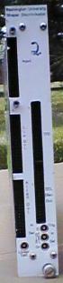
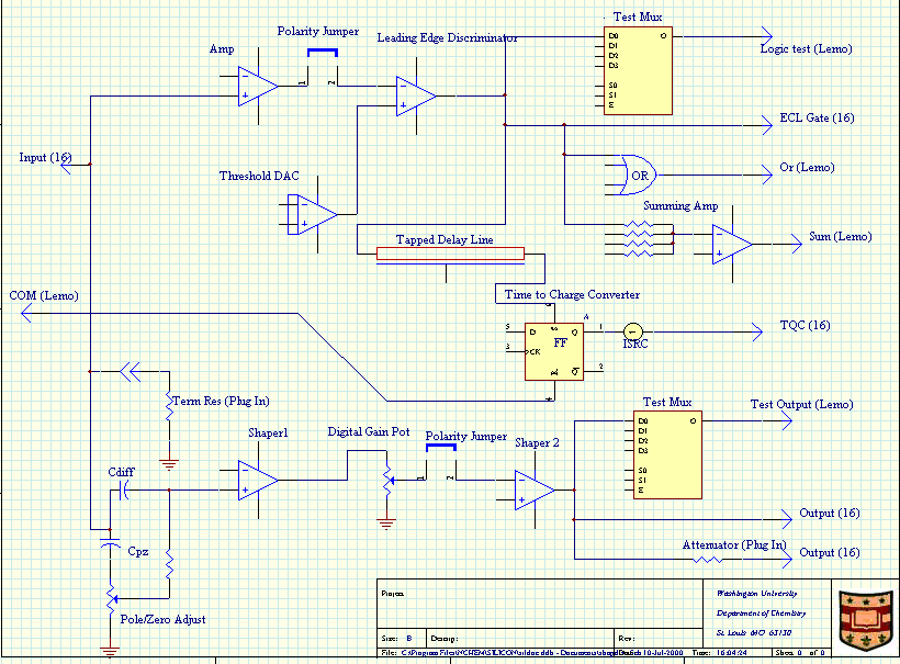
This unit contains 16 channels of computer-controlled leading edge discriminators with time-to-charge converters suitable for use with FERA and other charge-integrating ADCs. The TQCs can be configured as either common-start or common-stop. It also has 16 shapers with individually computer-controlled gains, and a test multiplexer that allows the user to inspect the logic and shaped signals from outside the detector cave or other remote location. These test outputs can be disabled on individual modules, such that several units can be or'd and summed to feed only one logic and one linear signal at a time to a scope for an entire array of detectors. Both the shapers and discriminators can be configured to accept either positive or negative going pulses, on a channel by channel basis. The discriminator produces individual outputs in ECL differential form on 34-pin ribbon-cable connectors, as well as an Or of all 16 channels on a Lemo NIM output. It also provides multiplicity as 50 mV/hit on a Lemo connector. The TDC outputs can be vetoed, to prevent starting TDC channels prematurely. Two shaped output are provided on 34-pin connectors. One of these outputs can be attenuated inside the unit by plug-in resistor packs. There are manual adjustments for Pole/Zero compensation of each channel, so that variations in preamp/detector shape can be compensated out of the shaped signal. The module occupies 2 slots in a standard CAMAC crate.
Block Diagram of the Silicon Shaper-Discriminator

Front Panel Connectors and indicators (left side - shaper):

Linear Test - Lemo Connector

This output can sample one of the shaper outputs for inspection. It can drive a 50 Ohm load. It introduces a slight DC offset and a slight loss of signal amplitude, so precision measurments should be made from the multi-pin outputs.

N - LED Indicator

This LED indicates that the shaper module is receiving commands from the CAMAC crate controller.

Sel - LED Indicator

This LED indicates that the Linear test output is presenting a signal for inspection.

Input - 34-Pin Male Connector

This is the input signal to the shaper and discriminator. It is terminated at 50 Ohms, unless other impedance is specified. Internal jumpers on the shaper and discriminator boards enable the signal to be of either polarity. The signal pins are to the left, normally the odd numbered contacts, starting with pin 1. Pins 33 and 34 are not used. The even contacts from 2 to 32 inclusive are ground.

Lin Out - 34-Pin Male Connector

This is the main shaper output. It is capable of driving a 50 Ohm load, and outputs over 8 volts of either polarity can be achieved. Pin assignment is as above.

Atten Out - 34-Pin Male Connector

This is an auxilliary attenuated output of the same shaper signals. 16-pin DIP resistor packs or solderable component headers can be placed in RP101 and RP901 to provide the desired attenuation ratio. This is calculated by Vout = Vin * Rl / (Rl + Rs) where Vin is the main shaper output, Rl is the termination resistance of the load on this output, and Rs is the series resistance of the resistor pack.

Front Panel Connectors and indicators (right side - discriminator):

Trig - LED Indicator

This red LED indicates that one of the discriminator channels has fired.

N - LED Indicator

This yellow LED indicates that the discriminator is receiving a command from the CAMAC crate controller.

Sel - LED Indicator

This green LED indicates that the discriminator is presenting one of the discriminator channel's logic signal to the front panel Disc Test jack.

Sum - Lemo Connector

This connector provides a multiplicity signal of -50 mV per channel hit.

Disc Test - Lemo Connector

This connector provides a discriminator logic signal at NIM standard levels for the selected channel.

Or - Lemo Connector

This connector provides a NIM standard logic signal that is an OR of all sixteen channels.

TFC Out - 34-Pin Male Connector

This connector provides a negative current source for each channel that is turned on by a start condition and turend off by a stop condition. An internal jumper on the discriminator board selects whether the TFC will operate in common-start or common-stop mode. The common start or stop is appled to the common start/stop connector on the back of the module. The function not controlled by the common signal comes from the discriminator for that channel. So, in common-stop mode, the start comes from the discriminator. There is a time delay, programmable in 20% steps from 0 to 100% by internal jumpers, that is applied to the individual start or stop signal, to allow a greater time resolution over a portion of the delay between the individual and common signals in cases where there is a great deal of dealy in the event trigger logic. The current that the TFC channel produces develops -40 mV into a 50 Ohm load. Even pins are ground, odd pins are the current source. This output was originally designed for the LeCroy FERA ADC, hence the name (time to FERA converter), but can be used with any charge integrating ADC that accepts negative signals.

ECL Disc Out - 34-Pin Male Connector

This output is an ECL differential logic signal that is the discriminator output. Pins 33 and 34 are not used. The odd pins are the true signals, the even pins are the complement signals.

Rear Panel Connectors:

Common Start/Stop - Lemo Connector

This connector accepts the NIM standard logic signal to start or stop the TFC current sources, as selected by the internal jumper.

Veto - Lemo Connector

This connector accepts a NIM standard logic signal to prevent the module from providing the OR output.

Block Diagram of the Silicon Shaper-Discriminator

CAMAC commands and programming:

Silicon Shaper

It is a bit intricate to program the gain setting because the chip used (a Dallas Semiconductor DS1267) uses a serial interface. We wanted to keep the hardware simple.

The test port is F=16, A=0
Only the lower 8 bits are used :
 bit #  7  6  5  4  3  2  1  0
        |  |  |  |  |  \_____/ =  Least significant 3 bits of channel address
        |  |  |  |  |
        |  |  |  |  ------------  1 if channel address <  8
        |  |  |  |
        |  |  |  ---------------  1 if channel address >= 8 
        |  x  x  (not used)
        |
        ------------------------  0 turns Module Select light on
If both bits 3 and 4 are zero, then the module ouputs no signal on the test port.

The Gain control register is F=16, A=1
The lower 3 bits are used :
 bit #  2   1   0
        |   |   |
        |   |   ----------------  The serial data stream
        |   |
        |   --------------------  The serial data clock
        |
        ------------------------  The 'RES/' control bit to the DS1267 Chip

The Dallas DS1267 Digital Pot chip has two separate 256-step pots on one chip. They can be connected together as one 512-step pot, but we did not set up our circuit board for that. So, with two pots each having 256 taps, we need 16 bits to control them, plus a bit for connecting the two together, Which we must set to 0 to keep the pots separate. There are 8 pot chips per module, so they need 136 bits to program them. (The serial data stream shifts through all 8 chips.) First the 'RES/' bit is put high (and it must be kept high for the entire process of loading the gains). The serial clock is put low (0). The 'stack-select' bit which connects the 2 pots together is shifted in first (as a 0 in bit # 0) then the serial clock is raised (1) and then lowered (0). The most significant bit of the gain for channel 15 is then put in bit # 0 and the clock is cycled 1 and then 0. This is repeated for the remaining 7 bits of channel 15, then the 8 bits of channel 14 are sent (most significant first). Then a stack select bit of 0 is sent, followed by the gain bits for channels 13 and 12. This process is repeated for all 16 channels, and after the bits for channel 0 are sent, the 'RES/' bit is set low. This loads the new gain setting into the pot's multiplexer circuit. So, you have to load the gain for all 16 channels in one stream, and then raise RES/, even if you are only changing one gain setting. I'm sorry this is so complex, but we were trying to keep the board simple.

Silicon Discriminator

The Discriminator is far simpler, traditional CAMAC style functions :
The test port is F=16, A=0
Only the lower 8 bits are used :
 bit #  7  6  5  4  3  2  1  0
        |  |  |  |  |  \_____/ =  Least significant 3 bits of channel address
        |  |  |  |  |
        |  |  |  |  ------------  0 if channel address <  8
        |  |  |  |
        |  |  |  ---------------  0 if channel address >= 8 
        |  x  x  (not used)
        |
        ------------------------  0 turns Module Select light on
If both bits 3 and 4 are one, then the module ouputs no signal on the test port.

The Threshold port is F=17, A=Chan # Only the lower 8 bits are used. A value of 0 is the smallest threshold, no matter the polarity of the signal. A value of 255 is the largest threshold.

Note that in a combined Shaper/Discriminator, separate CAMAC (N) addresses are used for the shaper and discriminator sections. Normally, the shaper is on the left (lower numbered slot) and the discriminator is on the right (higher numbered slot).

To Home