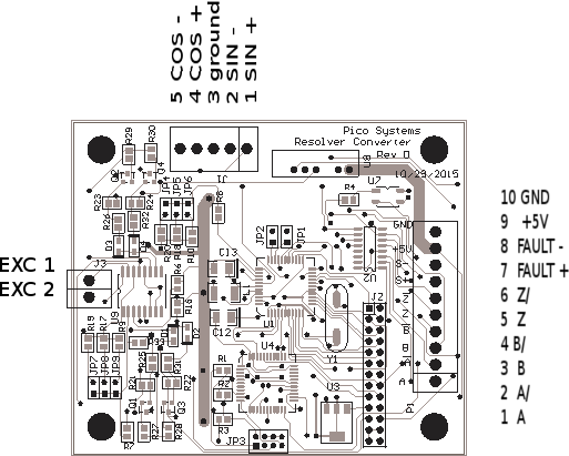
| P1 carries DC power, encoder signals and E-stop chain. Pin 1 is closest to the "P1" marking.
|
| Pin # | Signal |
| 1 | A+ |
| 2 | A- |
| 3 | B+ |
| 4 | B- |
| 5 | Z+ |
| 6 | Z- |
| 7 | ESTOP+ |
| 8 | ESTOP- |
| 9 | +5 V supply |
| 10 | Ground |
| A and B are the quadrature signals simulating the
encoder. Z is the index signal, a narrow pulse once
per revolution. If your encoder inputs are not differential,
just use the A+, B+ and Z+ outputs. If you don't need the
index function, just ignore the Z output.
|
J3 is the excitation output to the resolver. It is a differential
output of 4.0 to 28 V (differential), depending on jumper settings.
The jumpers should be set to give a peak reading (found by turning the
resolver shaft to maximize one output) of approximately 3.6 V p-p.
Pins are as follows :
| Pin # | Signal |
| 1 | Excitation+ |
| 2 | Excitation- |
|
J1 is the input from the resolver.
P4 Pins are as follows :
| Pin # | Signal |
| 1 | Sine+ |
| 2 | Sine- |
| 3 | Ground |
| 4 | Cosine+ |
| 5 | Cosine- |
| Amplitude selecting jumpers :
| JP4 & JP7 | JP5 & JP8 | JP6 & JP9 | Amplitude |
| X | X | X | 4.0 |
| . | X | X | 4.8 |
| X | . | X | 5.7 |
| . | . | X | 7.2 |
| X | X | . | 9.5 |
| . | X | . | 14.4 |
| X | . | . | 28.2 |
(X denotes jumper IN, . denotes jumper missing.)
 Board Layout Board Layout |
|
To Home
|